Section: New Results
Applications
Light diffusion in nanostructured optical fibers
Participants : Wilfried Blanc [Optical Fibers team, LPMC, Université Nice Sophia Antipolis, Nice] , Stéphane Lanteri, Paul Loriot, Claire Scheid.
Optical fibers are the basis for applications that have grown considerably in recent years (telecommunications, sensors, fiber lasers, etc.). Despite these undeniable successes, it is necessary to develop new generations of amplifying optical fibers that will overcome some limitations typical of silica. In this sense, the amplifying Transparent Glass Ceramics (TGC), and particularly the fibers based on this technology, open new perspectives that combine the mechanical and chemical properties of a glass host and the augmented spectroscopic properties of embedded nanoparticles, particularly rare earth-doped oxide nanoparticles. Such rare earth-doped silica-based optical fibers with transparent glass ceramic (TGC) core are fabricated by the Optical Fibers team of the Laboratory of Condensed Matter Physics (LPMC) in Nice. The objective of this collaboration with Wilfried Blanc at LPMC is the study of optical transmission terms of loss due to scattering through the numerical simulation of light propagation in a nanostructured optical fiber core using a high order DGTD method developed in the team.
Gap-plasmon confinement with gold nanocubes
Participants : Stéphane Lanteri, Antoine Moreau [Institut Pascal, Université Blaise Pascal] , Claire Scheid, Jonathan Viquerat.
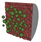
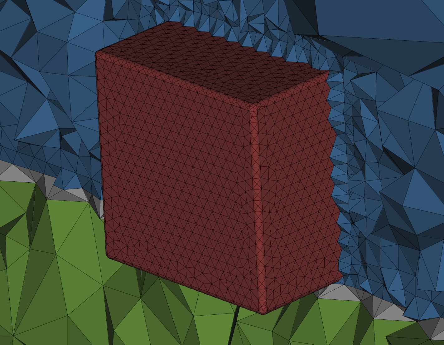
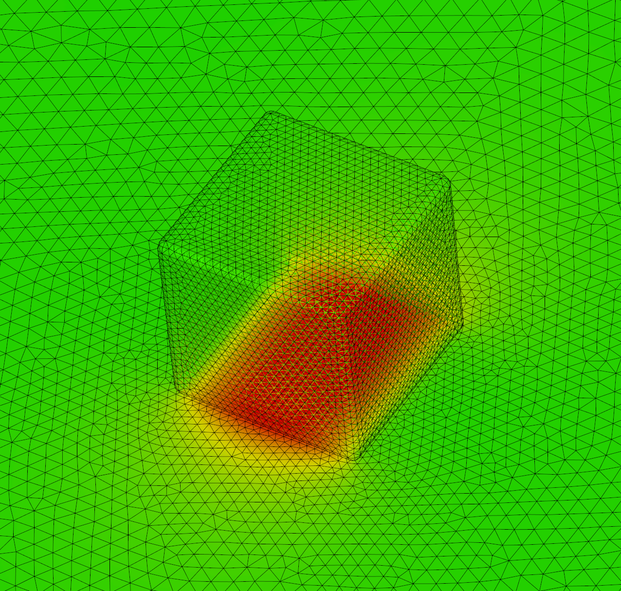
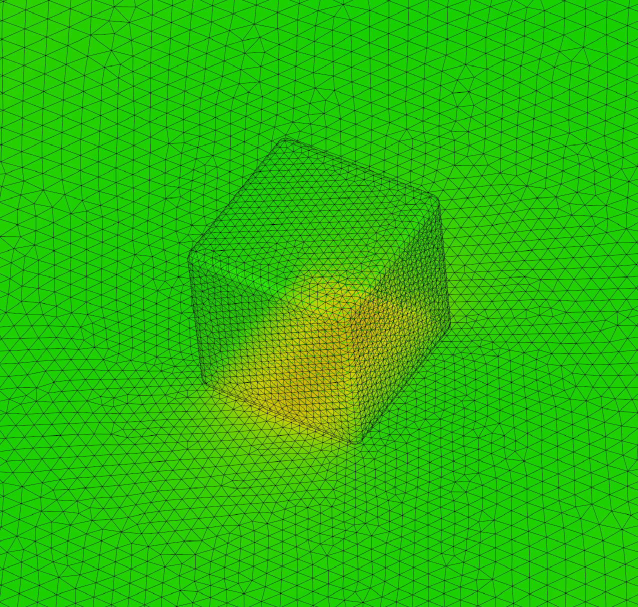
The propagation of light in a slit between metals is known to give rise to guided modes. When the slit is of nanometric size, plasmonic effects must be taken into account, since most of the mode propagates inside the metal. Indeed, light experiences an important slowing-down in the slit, the resulting mode being called gap-plasmon. Hence, a metallic structure presenting a nanometric slit can act as a light trap, i.e. light will accumulate in a reduced space and lead to very intense, localized fields. Recently, the chemical production of random arrangements of nanocubes on gold films at low cost was proved possible by Antoine Moreau and colleagues at Institut Pascal. Nanocubes are separated from the gold substrate by a dielectric spacer of variable thickness, thus forming a narrow slit under the cube. When excited from above, this configuration is able to support gap-plasmon modes which, once trapped, will keep bouncing back and forth inside the cavity. At visible frequencies, the lossy behavior of metals will cause the progressive absorption of the trapped electromagnetic field, turning the metallic nanocubes into efficient absorbers. The frequencies at which this absorption occurs can be tuned by adjusting the dimensions of the nanocube and the spacer. In collaboration with Antoine Moreau, we propose to study numerically the impact of the geometric parameters of the problem on the behaviour of a single nanocube placed over a metallic slab (see Fig. 8). The behavior of single nanocubes on metallic plates has been simulated, for lateral sizes ranging from 50 to 80 nm, and spacer thicknesses from 3 to 22 nm. The absorption efficiency in the cube at the resonance frequency is retrieved from the results of each computation (see Fig. 9).
|

|
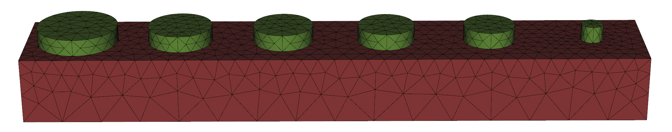
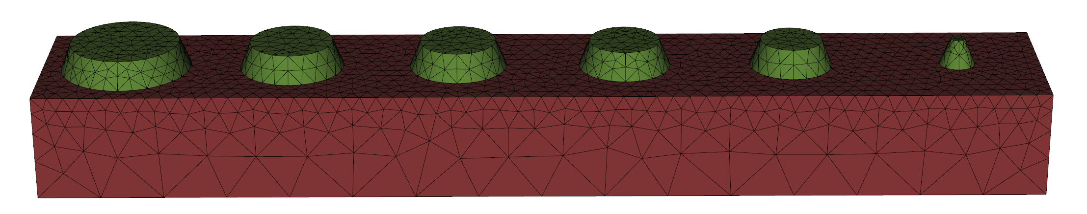
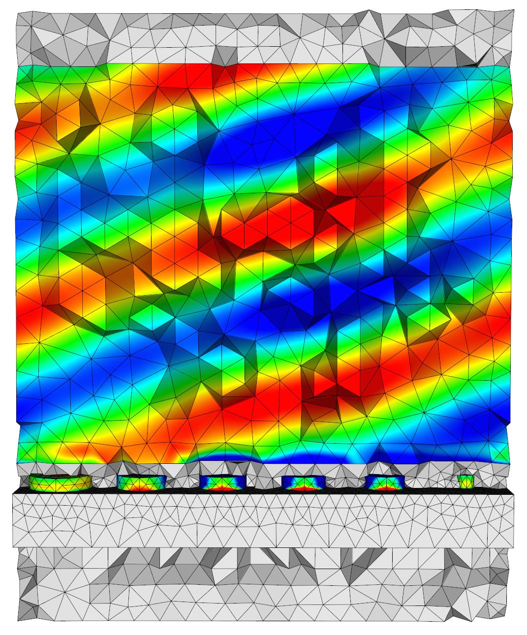
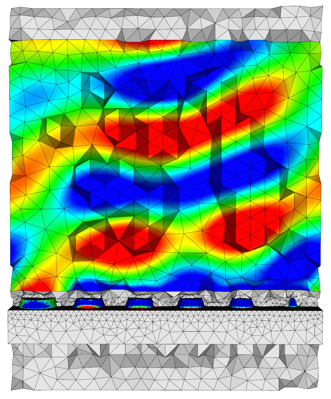
Dielectric reflectarrays
Participants : Maciej Klemm [Centre for Communications Research, University of Bristol] , Stéphane Lanteri, Claire Scheid, Jonathan Viquerat.
In the past few years, important efforts have been deployed to find alternatives to on-chip, low-performance metal interconnects between devices. Because of the ever-increasing density of integrated components, intra- and inter-chip data communications have become a major bottleneck in the improvement of information processing. Given the compactness and the simple implantation of the devices, communications via free-space optics between nanoantenna-based arrays have recently drawn more attention. Here, we focus on a specific low-loss design of dielectric reflectarray (DRA), whose geometry is based on a periodic repartition of dielectric cylinders on a metallic plate. When illuminated in normal incidence, specific patterns of such resonators provide a constant phase gradient along the dielectric/metal interface, thus altering the phase of the incident wavefront. The gradient of phase shift generates an effective wavevector along the interface, which is able to deflect light from specular reflection. However, the flaws of the lithographic production process can lead to discrepancies between the ideal device and the actual resonator array. Here, we propose to exploit our DGTD solver to study the impact of the lithographic flaws on the performance of a 1D reflectarray (see Fig. 10). Efficient computations are obtained by combining high-order polynomial approximation with curvilinear meshing of the resonators, yielding accurate results on very coarse meshes (see Fig. 11). The study is continued with the computation of the reflection of a 2D reflectarray. This work constitutes the base of a wider study in collaboration with Maciej Klemm at the Centre for Communications Research, University of Bristol.
|