Section: New Results
Applications
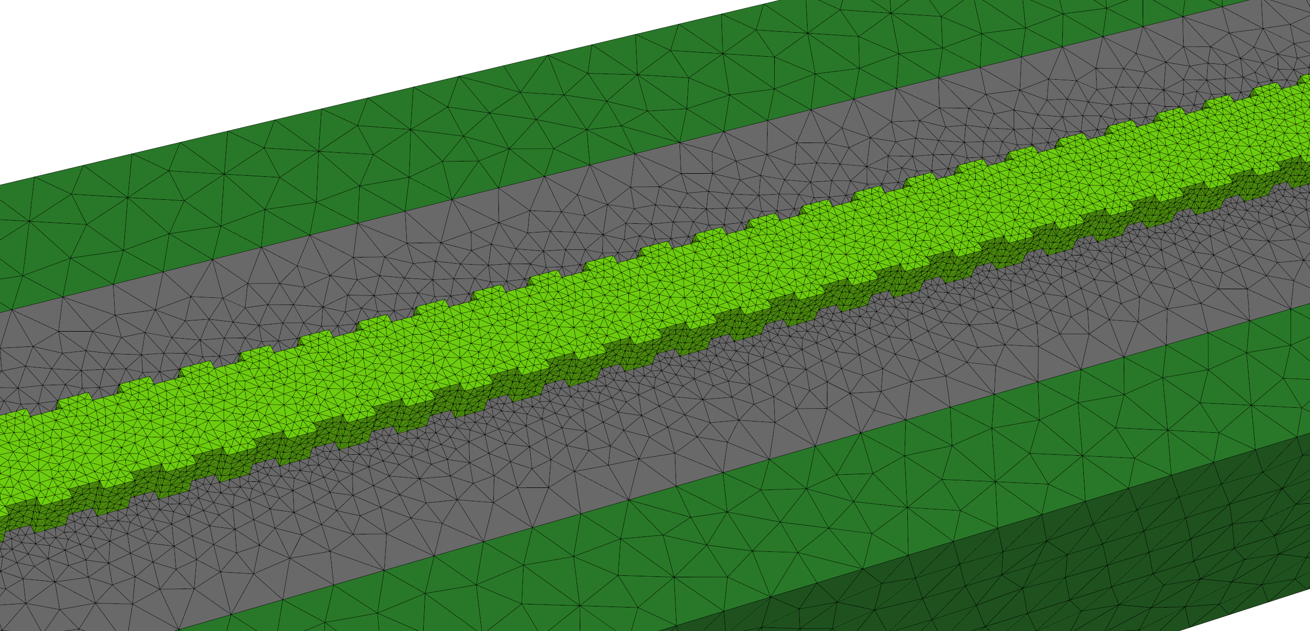
Light transmission in subwavelength gratings
Participants : Leandro Andrade Couto Fonseca, Hugo Enrique Hernandez Figueroa [Universidade Estadual de Campinas, Sao Paulo, Brazil] , Laurent Labonté [Information Quantique avec la Lumière et la Matière (QILM) team, INPHYNI, Université Nice Sophia Antipolis] , Stéphane Lanteri, Jonathan Viquerat.
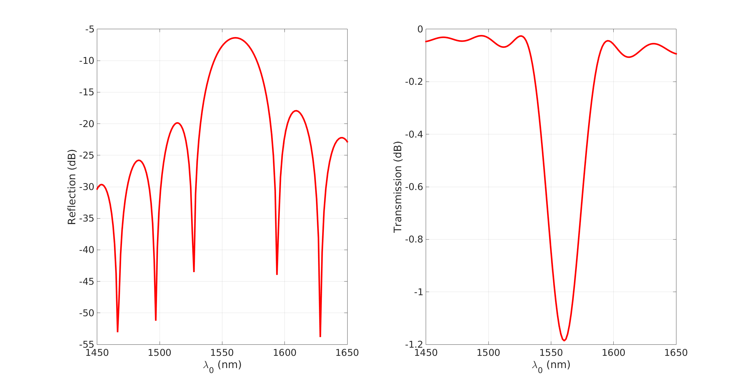
Silicon photonics has great potential to bringing together two technological areas that have transformed the last century, electronics and photonics. Silicon waveguides are important components for tailoring photonic functions on silicon. They have been studied extensively over the pas two decades. There are a number of waveguide geometries that have been developed in silicon. The most common are strip waveguides, rib waveguides and slot waveguides. The Bragg grating is a fundamental component in various optical devices and has applications in areas as diverse communications, laser and sensors. In the simplest configuration, a Bragg grating is a structure with periodic modulation of the effective refractive index. This modulation is commonly achieved by varying the refractive index (e.g. alternating material) or the physical dimensions of the waveguide. At each boundary, a reflection of the travelling light occurs, and the relative phase of the reflected signal is determined by the grating period and the wavelength. The repeated modulation of the refractive index results in multiple and distributed reflections. The reflected signals only interfere constructively in a narrow band around one particular wavelength, namely the Bragg wavelength. Within this range, light is strongly reflected. At other wavelengths, the multiple reflections interfere destructively and cancel each other out, and as a result, light is transmitted through the grating. This is the functional principle of the concept SubWavelength Gratings (SWG). In the context of the OPENING (On-chiP wirEless quantum state eNgineerING) project of the UCA JEDI Excellence Inititiave, we collaborate with the QILM team of the INPHYNI laboratory, on the numerical modeling of light propagation in SWG waveguides, suing a high order DGTD solver from the DIOGENeS software suite. Two situations are considered: (1) in a first step, an ideal configuration corresponding to a virtual design will be simulated; (2) in a second step, several deformed configurations, which are more in line with actual designs (i .e. from lithography), are studied with the goal of identifying the main sources of performance degradation from the transmission point of view.
|
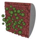
Light diffusion in nanostructured optical fibers
Participants : Wilfried Blanc [Optical Fibers team, INPHYNI, Université Nice Sophia Antipolis] , Stéphane Lanteri, Claire Scheid.
Optical fibers are the basis for applications that have grown considerably in recent years (telecommunications, sensors, fiber lasers, etc.). Despite these undeniable successes, it is necessary to develop new generations of amplifying optical fibers that will overcome some limitations typical of silica. In this sense, the amplifying Transparent Glass Ceramics (TGC), and particularly the fibers based on this technology, open new perspectives that combine the mechanical and chemical properties of a glass host and the augmented spectroscopic properties of embedded nanoparticles, particularly rare earth-doped oxide nanoparticles. Such rare earth-doped silica-based optical fibers with transparent glass ceramic (TGC) core are fabricated by the Optical Fibers team of the Laboratory of Condensed Matter Physics (INPHYNI) in Nice. The objective of this collaboration with Wilfried Blanc at LPMC is the study of optical transmission terms of loss due to scattering through the numerical simulation of light propagation in a nanostructured optical fiber core using a high order DGTD method developed in the team.
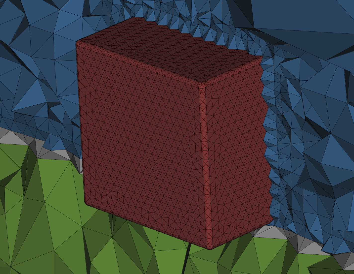
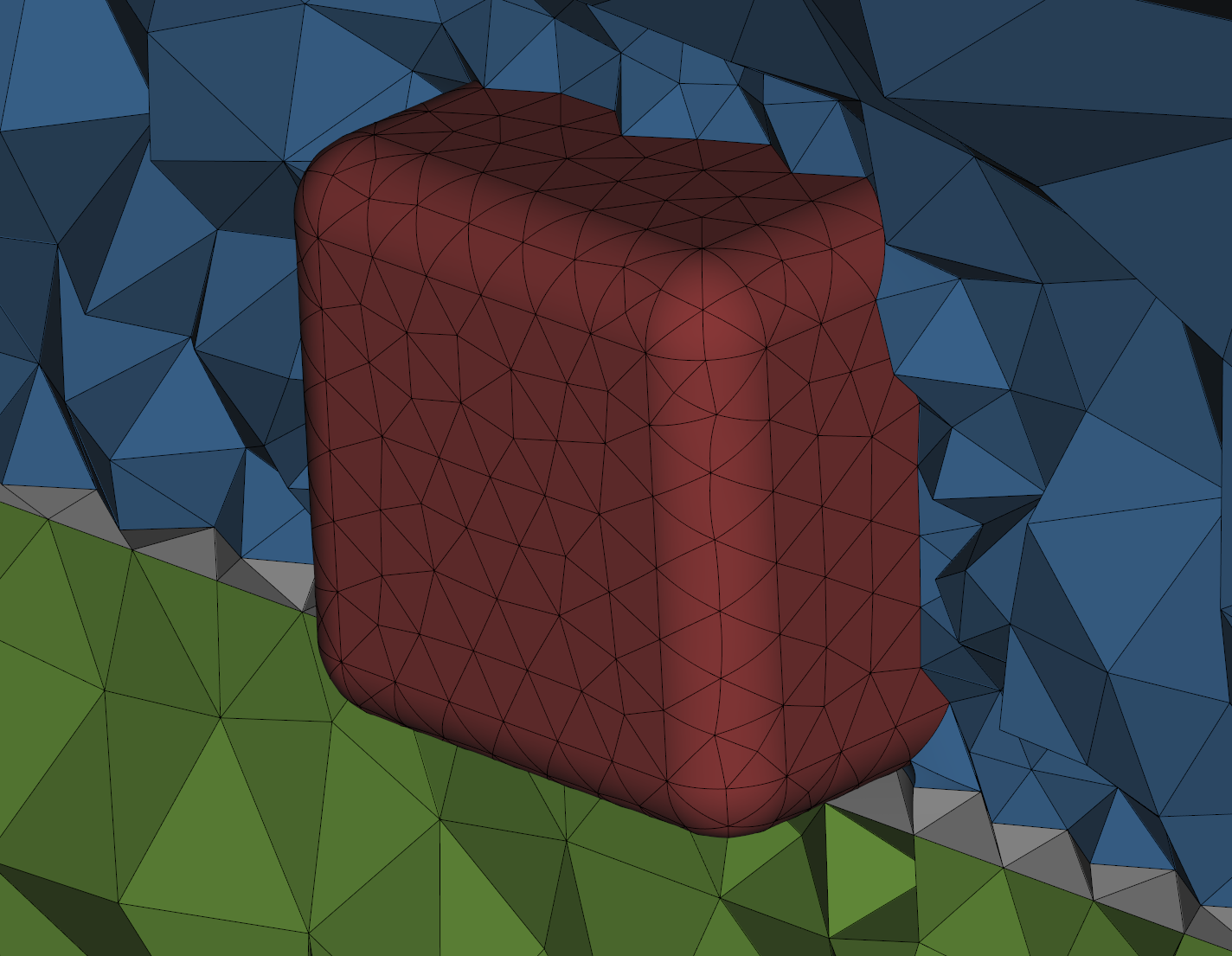
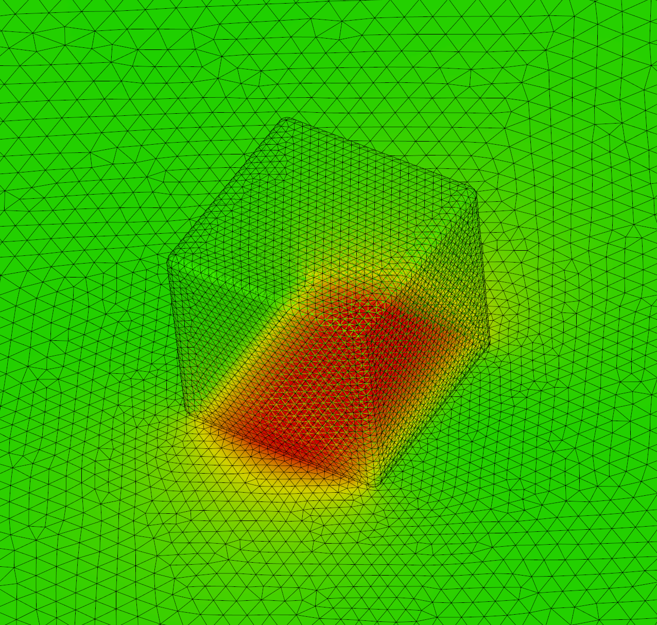
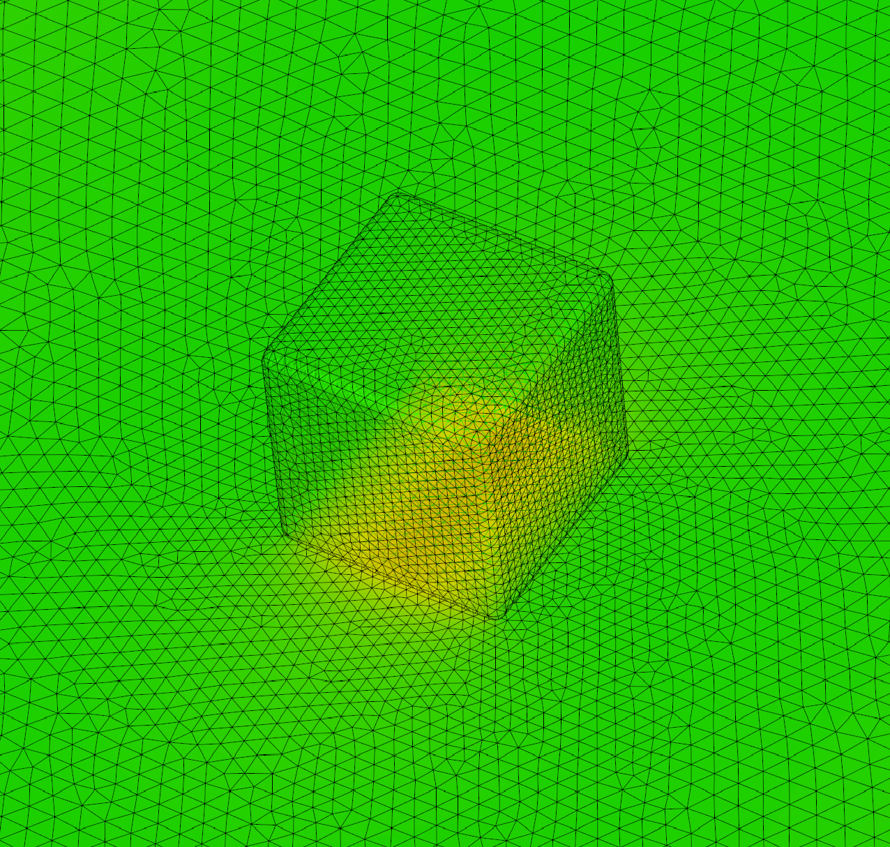
Gap-plasmon confinement with gold nanocubes
Participants : Stéphane Lanteri, Antoine Moreau [Institut Pascal, Université Blaise Pascal] , Armel Pitelet [Institut Pascal, Université Blaise Pascal] , Claire Scheid, Nikolai Schmitt, Jonathan Viquerat.
The propagation of light in a slit between metals is known to give rise to guided modes. When the slit is of nanometric size, plasmonic effects must be taken into account, since most of the mode propagates inside the metal. Indeed, light experiences an important slowing-down in the slit, the resulting mode being called gap-plasmon. Hence, a metallic structure presenting a nanometric slit can act as a light trap, i.e. light will accumulate in a reduced space and lead to very intense, localized fields. Recently, the chemical production of random arrangements of nanocubes on gold films at low cost was proved possible by Antoine Moreau and colleagues at Institut Pascal. Nanocubes are separated from the gold substrate by a dielectric spacer of variable thickness, thus forming a narrow slit under the cube. When excited from above, this configuration is able to support gap-plasmon modes which, once trapped, will keep bouncing back and forth inside the cavity. At visible frequencies, the lossy behavior of metals will cause the progressive absorption of the trapped electromagnetic field, turning the metallic nanocubes into efficient absorbers. The frequencies at which this absorption occurs can be tuned by adjusting the dimensions of the nanocube and the spacer. In collaboration with Antoine Moreau, we propose to study numerically the impact of the geometric parameters of the problem on the behaviour of a single nanocube placed over a metallic slab (see Fig. 9). The behavior of single nanocubes on metallic plates has been simulated, for lateral sizes ranging from 50 to 80 nm, and spacer thicknesses from 3 to 22 nm. The absorption efficiency in the cube at the resonance frequency is retrieved from the results of each computation (see Fig. 10).
|
|
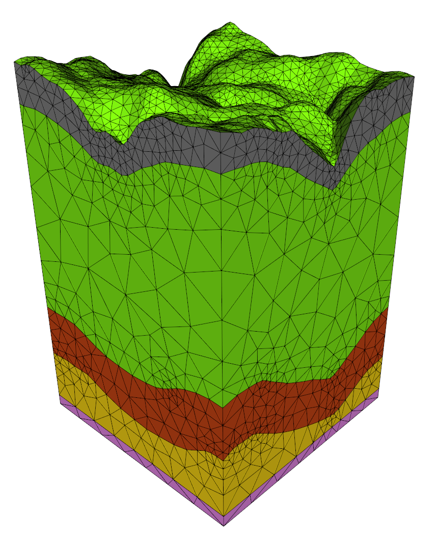
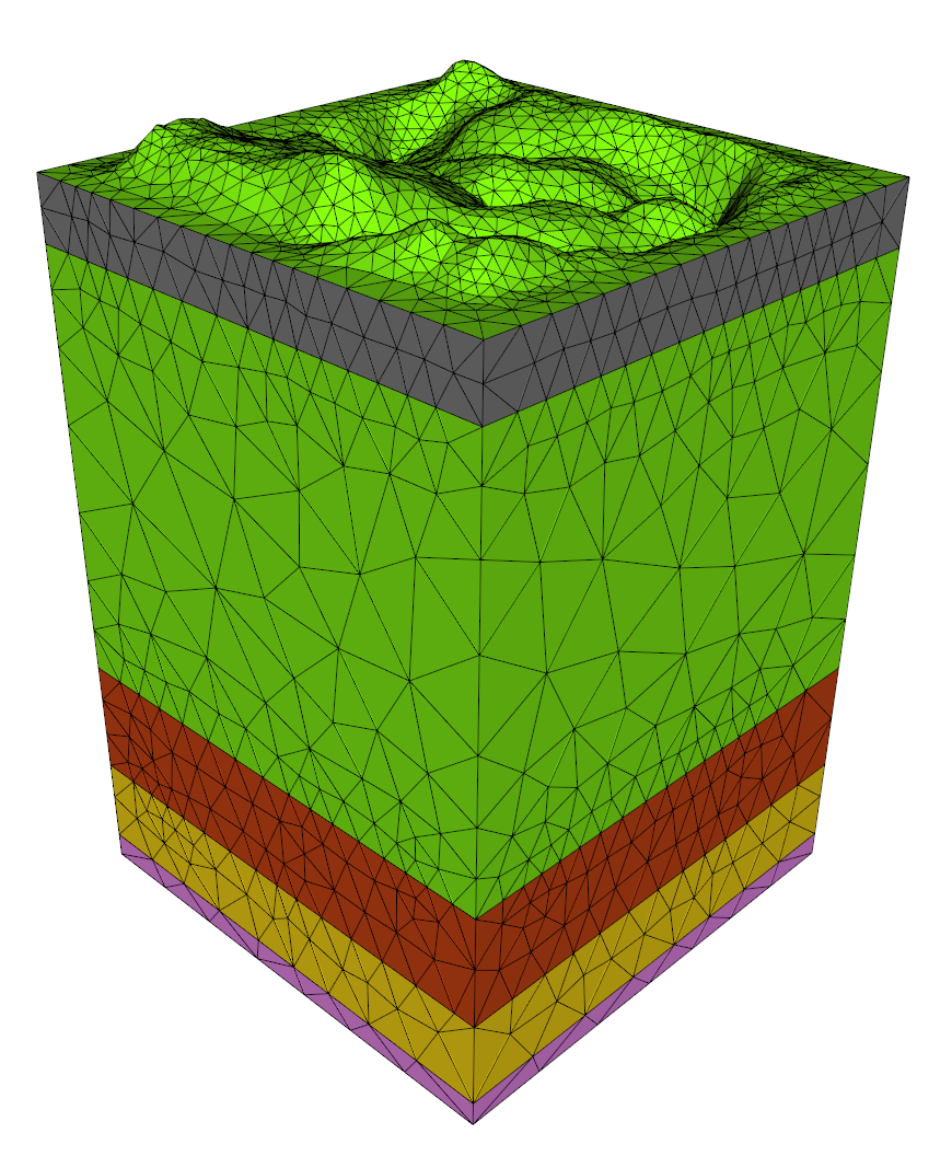
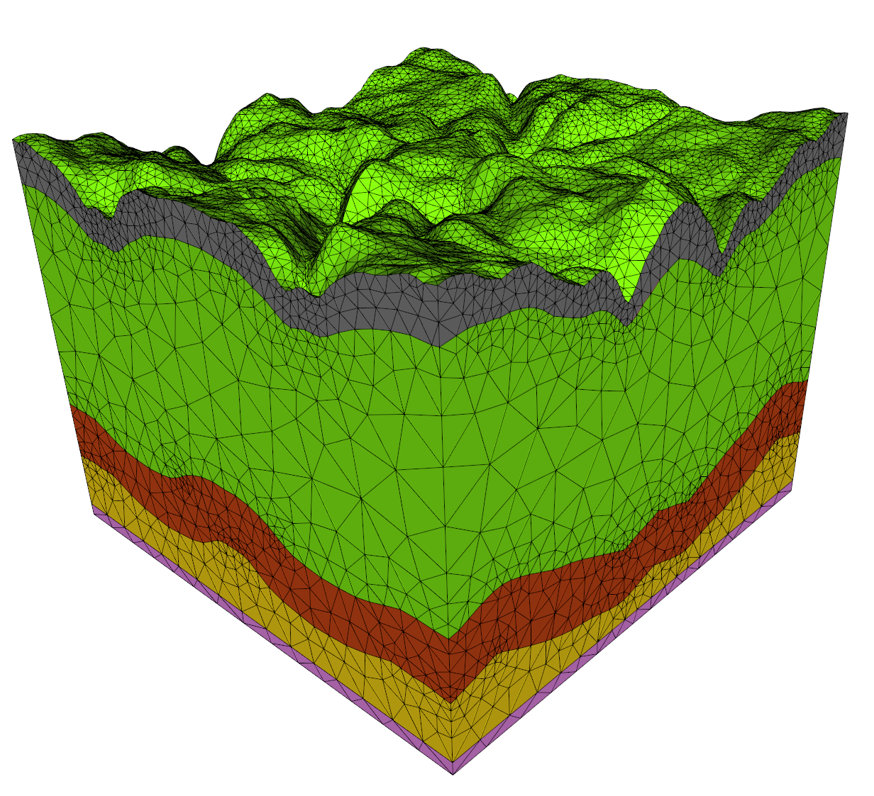
Light-trapping in nanostructured solar cells
Participants : Urs Aeberhard [IEK5 - Photovoltaik, Forschungszentrum Juelich GmbH, German] , Karsten Bittkau [IEK5 - Photovoltaik, Forschungszentrum Juelich GmbH, German] , Alexis Gobé, Stéphane Lanteri.
This work is undertaken in the context of the EoCoE Center of Excellence in collaboration with researchers from IEK5 - Photovoltaik, Forschungszentrum Juelich GmbH, Germany. The objective is to design a scalable high order DGTD solver for the simulation of light trapping in a multi-layer solar cell with surface texture. For that purpose, we rely on the DIOGENeS software suite from which we extract a high order DGTD solver for the problem under consideration, taking into account its specificities (in particular, with regards to material models and boundary conditions). We also need to specify and develop a dedicated preprocessing tool for building topography conforming geometrical models. Simulations are performed on the Occigen PRACE system at CINES.