

Section: New Results
Applications
Gap-plasmon confinement with gold nanocubes
Participants : Stéphane Lanteri, Antoine Moreau [Institut Pascal, Université Blaise Pascal] , Armel Pitelet [Institut Pascal, Université Blaise Pascal] , Claire Scheid, Nikolai Schmitt, Jonathan Viquerat.
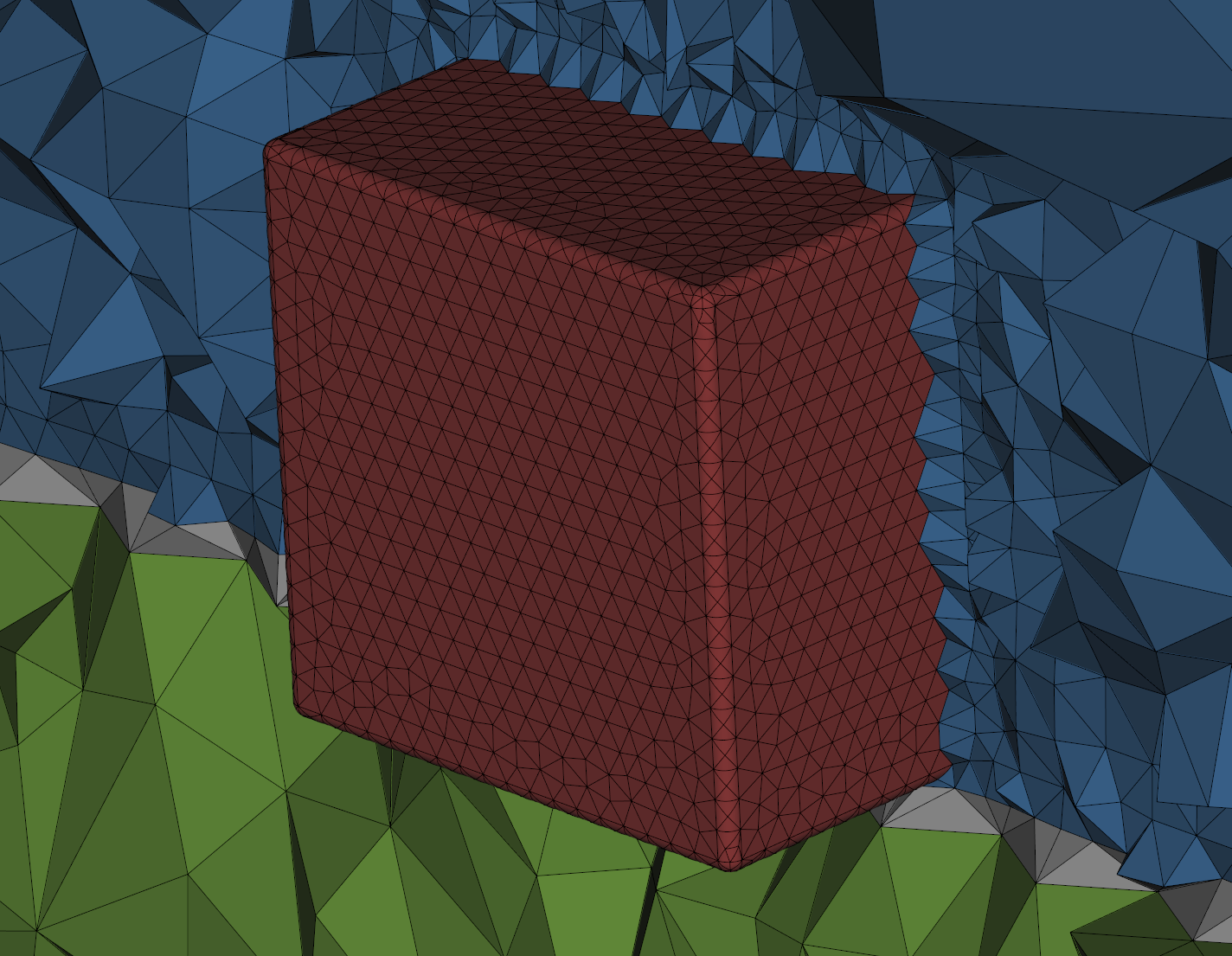
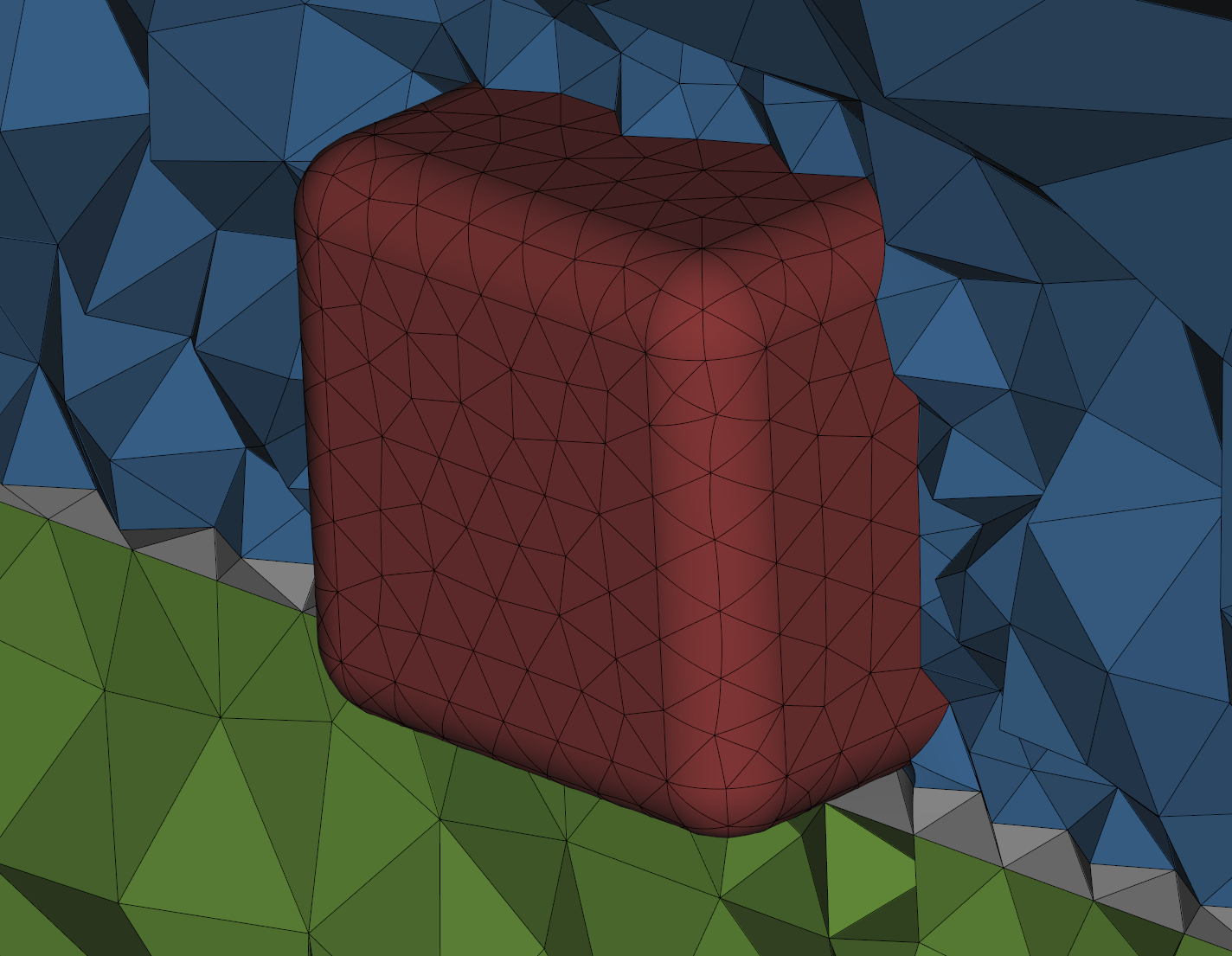
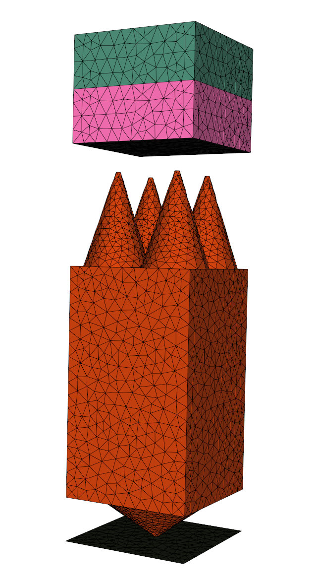
The propagation of light in a slit between metals is known to give rise to guided modes. When the slit is of nanometric size, plasmonic effects must be taken into account, since most of the mode propagates inside the metal. Indeed, light experiences an important slowing-down in the slit, the resulting mode being called gap-plasmon. Hence, a metallic structure presenting a nanometric slit can act as a light trap, i.e. light will accumulate in a reduced space and lead to very intense, localized fields. Recently, the chemical production of random arrangements of nanocubes on gold films at low cost was proved possible by Antoine Moreau and colleagues at Institut Pascal. Nanocubes are separated from the gold substrate by a dielectric spacer of variable thickness, thus forming a narrow slit under the cube. When excited from above, this configuration is able to support gap-plasmon modes which, once trapped, will keep bouncing back and forth inside the cavity. At visible frequencies, the lossy behavior of metals will cause the progressive absorption of the trapped electromagnetic field, turning the metallic nanocubes into efficient absorbers. The frequencies at which this absorption occurs can be tuned by adjusting the dimensions of the nanocube and the spacer. In collaboration with Antoine Moreau, we propose to study numerically the impact of the geometric parameters of the problem on the behaviour of a single nanocube placed over a metallic slab (see Fig. 9).
|
Photovoltaics
The ultimate success of photovoltaic (PV) cell technology requires substantial progress in both cost reduction and efficiency improvement. An actively studied approach to simultaneously achieve these two objectives is to leverage light trapping schemes. Light trapping allows solar cells to absorb sunlight using an active material layer that is much thinner than the material’s intrinsic absorption length. This then reduces the amount of materials used in PV cells, which cuts cell cost in general, and moreover facilitates mass production of PV cells that are based on less abundant materials. In addition, light trapping can improve cell efficiency, since thinner cells provide better collection of photo-generated charge carriers. Enhancing the light absorption in ultrathin film silicon solar cells is thus of paramount importance for improving efficiency and reducing cost. We are involved in several studies in collaboration with physicists that aim at simulating light trapping in complex solar cell structures using high order DG and HDG solvers developed in our core research activities.
Light-trapping in texturized thin film solar cells
Participants : Urs Aeberhard [IEK5 - Photovoltaik, Forschungszentrum Juelich GmbH, German] , Karsten Bittkau [IEK5 - Photovoltaik, Forschungszentrum Juelich GmbH, German] , Alexis Gobé, Stéphane Lanteri.
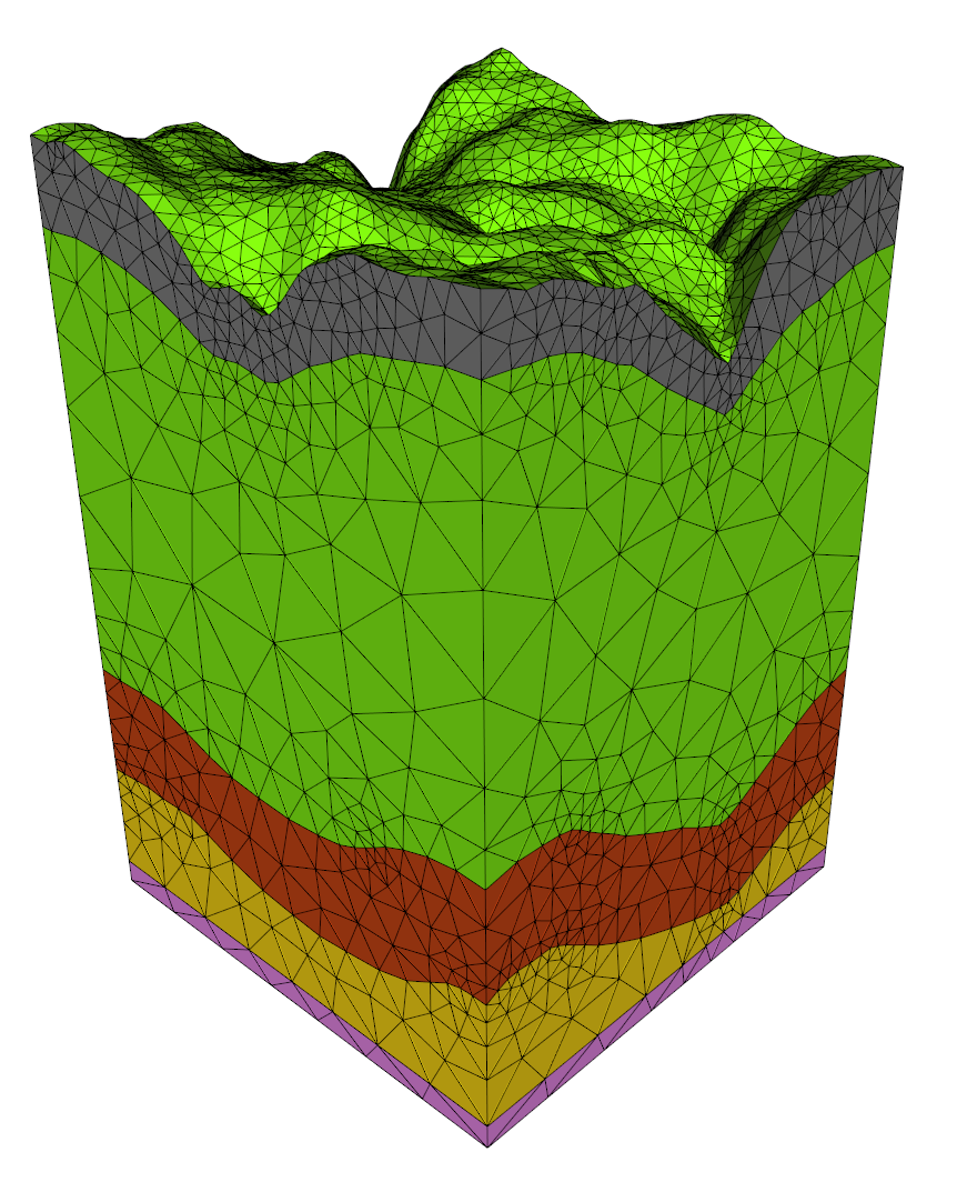
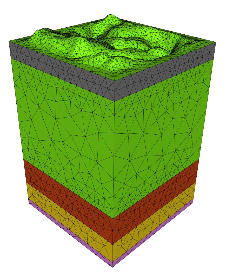
This work is undertaken in the context of the EoCoE Center of Excellence in collaboration with researchers from IEK5 - Photovoltaik, Forschungszentrum Juelich GmbH, Germany. The objective is to design a scalable high order DGTD solver for the simulation of light trapping in a multi-layer solar cell with surface texture. For that purpose, we rely on the DIOGENeS software suite from which we extract a high order DGTD solver for the problem under consideration, taking into account its specificities (in particular, with regards to material models and boundary conditions). We also need to specify and develop a dedicated preprocessing tool for building topography conforming geometrical models. Simulations are performed on the Occigen PRACE system at CINES.
|
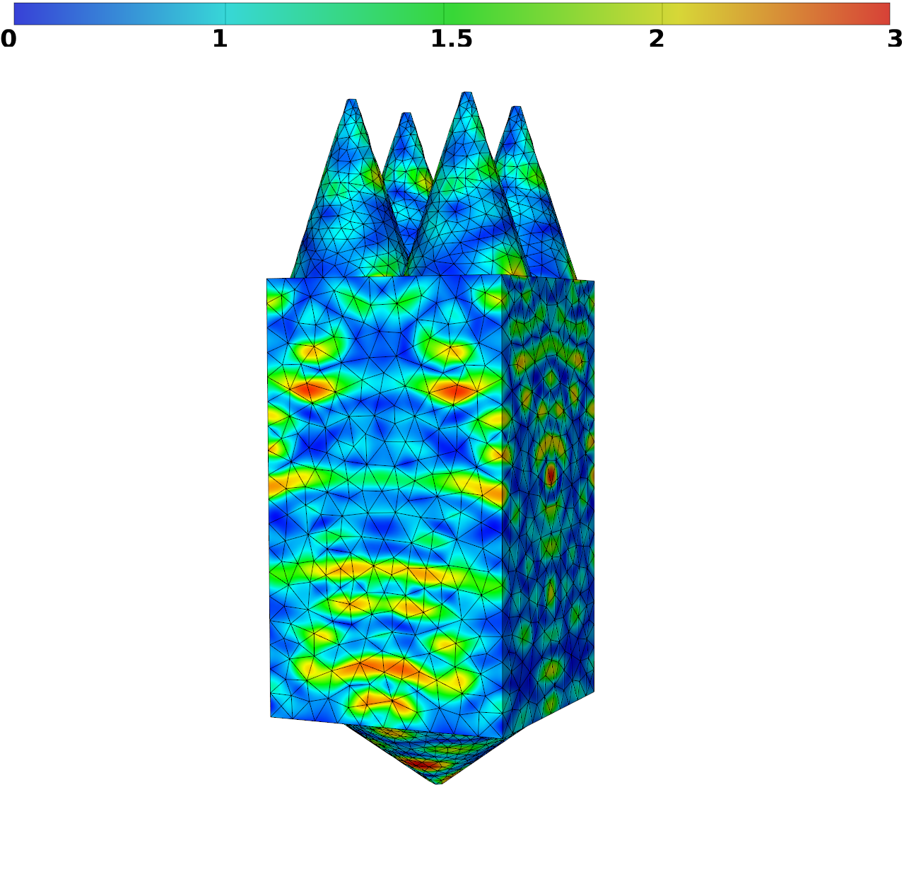
Light-trapping in nanocone gratings
Participants : Stéphane Collin [Sunlit team, C2N-CNRS, Marcoussi] , Alexis Gobé, Julie Goffard [Sunlit team, C2N-CNRS, Marcoussi] , Stéphane Lanteri.
There is significant recent interest in designing ultrathin crystalline silicon solar cells with active layer thickness of a few micrometers. Efficient light absorption in such thin films requires both broadband antireflection coatings and effective light trapping techniques, which often have different design considerations. In collaboration with physicists from the Sunlit team at C2N-CNRS, we conduct a numerical study of solar cells based on nanocone gratings. Indeed, it has been previously shown that by employing a double-sided grating design, one can separately optimize the geometries for antireflection and light trapping purposes to achieve broadband light absorption enhancement [47]. In the present study, we adopt the nanocone grating considered in [47]. This structure contains a crystalline silicon thin film with nanocone gratings also made of silicon. The circular nanocones form two-dimensional square lattices on both the front and the back surfaces. The film is placed on a perfect electric conductor (PEC) mirror. The ultimate objective of this study is to devise a numerical optimization strategy to infer optimal values of the geometrical characteristics of the nanocone grating on each side of the crystalline silicon thin film. Absorption characteristics are here evaluated using the high order DGTD solver from the DIOGENeS software suite.
|
Inver design of metasurfaces
Participants : Régis Duvigneau [ACUMES project-team, Inria Sophia Antipolis-Méditerranée] , Mahmoud Elsawy, Patrice Genevet [CRHEA laboratory, Sophia Antipolis] , Stéphane Lanteri.
Metasurfaces are flat surfaces consisting of sub-wavelength nanoresonators, made of plasmonic or high dielectric refractive index materials patterned in a specific way. These flat surfaces provide nearly full control of the light properties in a very short propagation distance with high resolution. By changing the dimensions, shapes, and orientation of these nanoresonators, different functionalities can be obtained. The complexity of the problem and the wide parameter space, make the direct modelling problem insufficient. Recently, several optimization techniques have been applied to the field of nanophotonics (including metasurfaces) by solving an inverse design problem. Generally speaking, there are two classes of optimization techniques that have been used in the metasurface designs; local and global techniques. The local methods depend on the initial guess and most of them require the computation of the gradient, which might be challenging. In addition, they are limited to small parameter space. On the other hand, global optimization techniques are suitable for optimizing several parameters moreover, they do not stuck in a local minima/maxima like the local methods. However, most of the global techniques used in the metasurface designs require costly simulations (for large parameter space), which make them inapplicable for modeling real-life designs that require 3D fullwave solvers. In this study conducted in collaboration with physicists at CRHEA, we use two efficient global optimization techniques based on statistical learning in order to overcome the disadvantageous of usual global optimization methods. The first one is the covariance matrix adaptation evolutionary strategy (CMA-ES). The CMA-ES has been gaining a lot of attention since it requires fewer cost function evaluations compared to the other evolutionary algorithms like genetic algorithms especially for 3D problems that require expensive simulations even with the high-performance computational resources. The second method is the Efficient Global Optimization (EGO) algorithm. The EGO algorithm is based on the surrogate modelling, that is to say, replacing the complex or costly evaluation process by a simpler and cheaper model to reduce dramatically the computational cost (number of calls for the electromagnetic simulations). Both techniques are offered by the Famosa library (http://famosa.gforge.inria.fr), which is developed by R. Duvigneau and colleagues in the ACUMES project-team.