

Section: New Results
Applications
Inverse design of metasurfaces using statistical learning methods
Participants : Régis Duvigneau [ACUMES project-team, Inria Sophia Antipolis-Méditerranée] , Mahmoud Elsawy, Patrice Genevet [CRHEA laboratory, Sophia Antipolis] , Stéphane Lanteri.
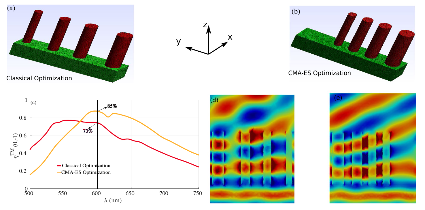
Metasurfaces are flat optical nanocomponents, that are the basis of several more complicated optical devices. The optimization of their performance is thus a crucial concern, as they impact a wide range of applications. Yet, current design techniques are mostly based on engineering knowledge, and may potentially be improved by a rigorous analysis based on accurate simulation of Maxwell's equations. The goal of this study is to optimize phase gradient metasurfaces by taking advantage of our fullwave high order Discontinuous Galerkin time-Domain solver implemented in DIOGENeS, coupled with two advanced optimization techniques based on statistical learning and evolutionary strategies. Our key findings are novel designs for Gan semiconductor phase gradient metasurfaces operating at visible wavelengths. Our numerical results reveal that rectangular and cylindrical nanopillar arrays can achieve more than respectively 88% and 85% of diffraction efficiency for TM polarization and both TM and TE polarization respectively, using only 150 fullwave simulations. To the best of our knowledge, this is the highest blazed diffraction efficiency reported so far at visible wavelength using such metasurface architectures. Fig. 8 depicts the superiority of the proposed statistical learning approaches over standard gradient-based optimization strategies. This work has been recently published [22].
|
Optimization of light-trapping in nanocone gratings
Participants : Stéphane Collin [Sunlit team, C2N-CNRS, Marcoussi] , Alexis Gobé, Julie Goffard [Sunlit team, C2N-CNRS, Marcoussi] , Stéphane Lanteri.
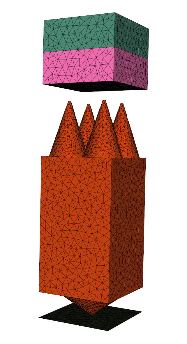
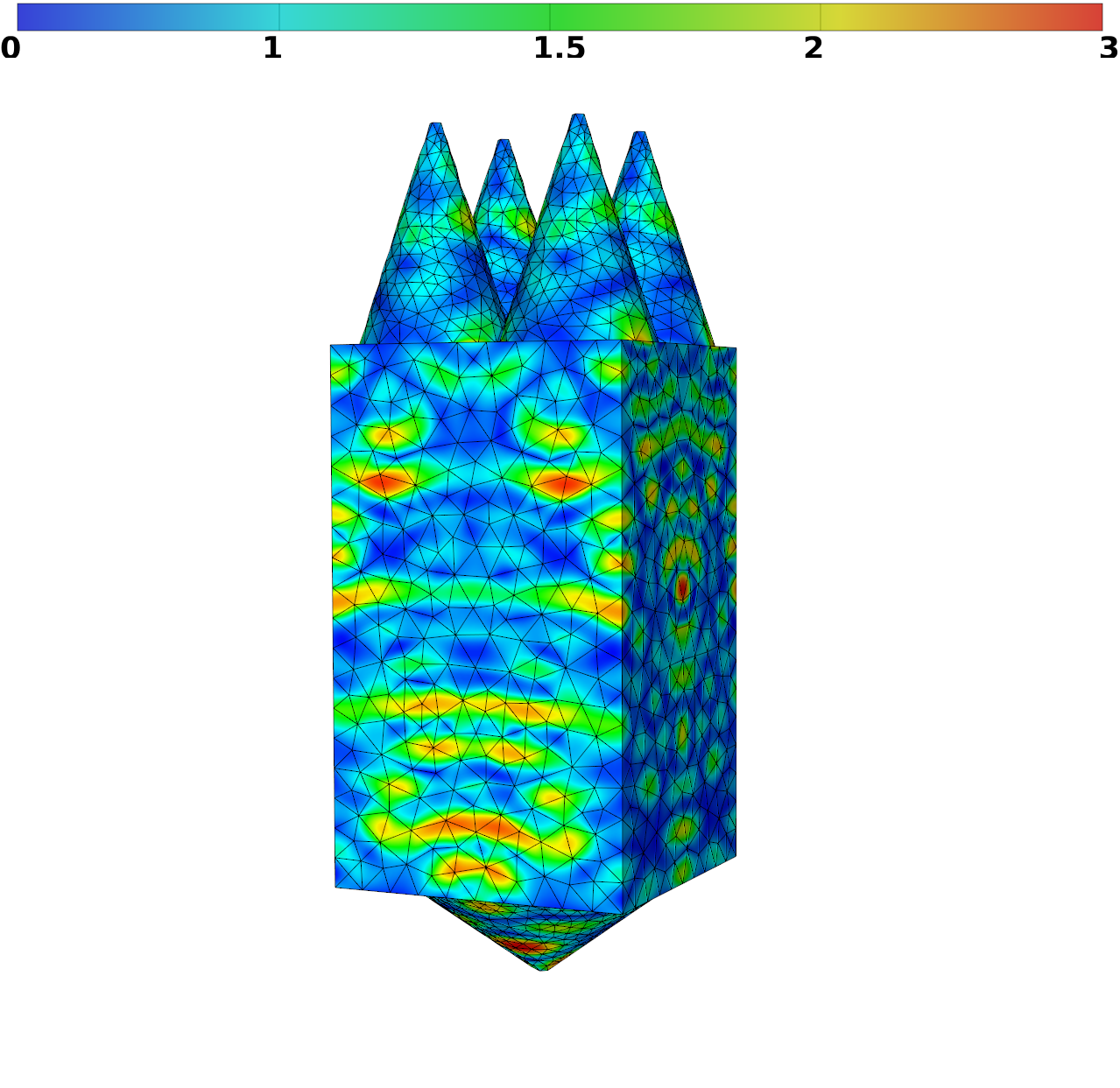
There is significant recent interest in designing ultrathin crystalline silicon solar cells with active layer thickness of a few micrometers. Efficient light absorption in such thin films requires both broadband antireflection coatings and effective light trapping techniques, which often have different design considerations. In collaboration with physicists from the Sunlit team at C2N-CNRS, we conduct a numerical study of solar cells based on nanocone gratings. Indeed, it has been previously shown that by employing a double-sided grating design, one can separately optimize the geometries for antireflection and light trapping purposes to achieve broadband light absorption enhancement [60]. In the present study, we adopt the nanocone grating considered in [60]. This structure contains a crystalline silicon thin film with nanocone gratings also made of silicon. The circular nanocones form two-dimensional square lattices on both the front and the back surfaces. The film is placed on a perfect electric conductor (PEC) mirror. The ultimate objective of this study is to devise a numerical optimization strategy to infer optimal values of the geometrical characteristics of the nanocone grating on each side of the crystalline silicon thin film. Absorption characteristics are here evaluated using the high order DGTD solver from the DIOGENeS software suite. We use two efficient global optimization techniques based on statistical learning to adpat the geometrical characteristics of the nanocones in order the maximize the light absorption properties of this type of solr cells.
|
Influence of spatial dispersion on surface plasmons and grating couplers
Participants : Stéphane Lanteri, Antoine Moreau [Institut Pascal, Université Blaise Pascal] , Armel Pitelet [Institut Pascal, Université Blaise Pascal] , Claire Scheid, Nikolai Schmitt, Jonathan Viquerat.
Recent experiments have shown that spatial dispersion may have a conspicuous impact on the response of plasmonic structures. This suggests that in some cases the Drude model should be replaced by more advanced descriptions that take spatial dispersion into account, like the hydrodynamic model. Here we show that nonlocality in the metallic response affects surface plasmons propagating at the interface between a metal and a dielectric with high permittivity. As a direct consequence, any nanoparticle with a radius larger than 20 nm can be expected to be sensitive to spatial dispersion whatever its size. The same behavior is expected for a simple metallic grating allowing the excitation of surface plasmons, just as in Woods famous experiment. Finally, we carefully set up a procedure to measure the signature of spatial dispersion precisely, leading the way for future experiments. Importantly, our work suggests that for any plasmonic structure in a high permittivity dielectric, nonlocality should be taken into account.
Optimization and uncertainty quantification of gradient index metasurfaces
Participants : Gauthier Brière [CRHEA laboratory, Sophia Antipolis] , Herbert de Gersem [TEMF institute, TU Darmstadt, Germany] , Patrice Genevet [CRHEA laboratory, Sophia Antipolis] , Niklas Georg [TEMF institute, TU Darmstadt, Germany] , Stéphane Lanteri, Dimitrios Loukrezis [TEMF institute, TU Darmstadt, Germany] , Ulrich Römer [TEMF institute, TU Darmstadt, Germany] , Nikolai Schmitt.
The design of intrinsically flat two-dimensional optical components, i.e., metasurfaces, generally requires an extensive parameter search to target the appropriate scattering properties of their constituting building blocks. Such design methodologies neglect important near-field interaction effects, playing an essential role in limiting the device performance. Optimization of transmission, phase-addressing and broadband performances of metasurfaces require new numerical tools. Additionally, uncertainties and systematic fabrication errors should be analysed. These estimations, of critical importance in the case of large production of metaoptics components, are useful to further project their deployment in industrial applications. Here, we report on a computational methodology to optimize metasurface designs. We complement this computational methodology by quantifying the impact of fabrication uncertainties on the experimentally characterized components. This analysis provides general perspectives on the overall metaoptics performances, giving an idea of the expected average behavior of a large number of devices.