Section: Application Domains
Computational electromagnetics
Electromagnetic devices are ubiquitous in present day technology. Indeed, electromagnetism has found and continues to find applications in a wide array of areas, encompassing both industrial and societal purposes. Applications of current interest include (among others) those related to communications (e.g transmission through optical fiber lines), to biomedical devices (e.g microwave imaging, micro-antenna design for telemedecine, etc.), to circuit or magnetic storage design (electromagnetic compatibility, hard disc operation), to geophysical prospecting, and to non-destructive evaluation (e.g crack detection), to name but just a few. Equally notable and motivating are applications in defence which include the design of military hardware with decreased signatures, automatic target recognition (e.g bunkers, mines and buried ordnance, etc.) propagation effects on communication and radar systems, etc. Although the principles of electromagnetics are well understood, their application to practical configurations of current interest, such as those that arise in connection with the examples above, is significantly complicated and far beyond manual calculation in all but the simplest cases. These complications typically arise from the geometrical characteristics of the propagation medium (irregular shapes, geometrical singularities), the physical characteristics of the propagation medium (heterogeneity, physical dispersion and dissipation) and the characteristics of the sources (wires, etc.).
Part of the activities of the NACHOS project-team aim at the development of high performance, high order, unstructured mesh based solvers for the full system of Maxwell equations, in the time domain and frequency domain regimes. Although many of the above-mentioned electromagnetic wave propagation problems can potentially benefit from the proposed numerical methodologies, the team concentrates its efforts on the following two situations.
Interaction of electromagnetic waves with biological tissues at microwave frequencies.
Two main reasons motivate our commitment to consider this type of problem for the application of the numerical methodologies developed in the NACHOS project-team:
-
First, from the numerical modeling point of view, the interaction between electromagnetic waves and biological tissues exhibit the three sources of complexity identified previously and are thus particularly challenging for pushing one step forward the state-of-the art of numerical methods for computational electromagnetics. The propagation media is strongly heterogeneous and the electromagnetic characteristics of the tissues are frequency dependent. Interfaces between tissues have rather complicated shapes that cannot be accurately discretized using cartesian meshes. Finally, the source of the signal often takes the form of a complicated device (e.g a mobile phone or an antenna array).
-
Second, the study of the interaction between electromagnetic waves and living tissues is of interest to several applications of societal relevance such as the assessment of potential adverse effects of electromagnetic fields or the utilization of electromagnetic waves for therapeutic or diagnostic purposes. It is widely recognized nowadays that numerical modeling and computer simulation of electromagnetic wave propagation in biological tissues is a mandatory path for improving the scientific knowledge of the complex physical mechanisms that characterize these applications.
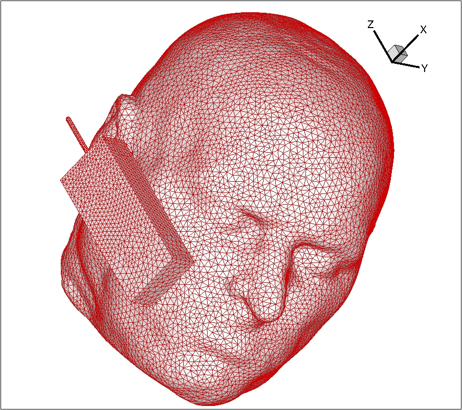
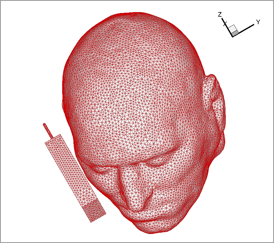
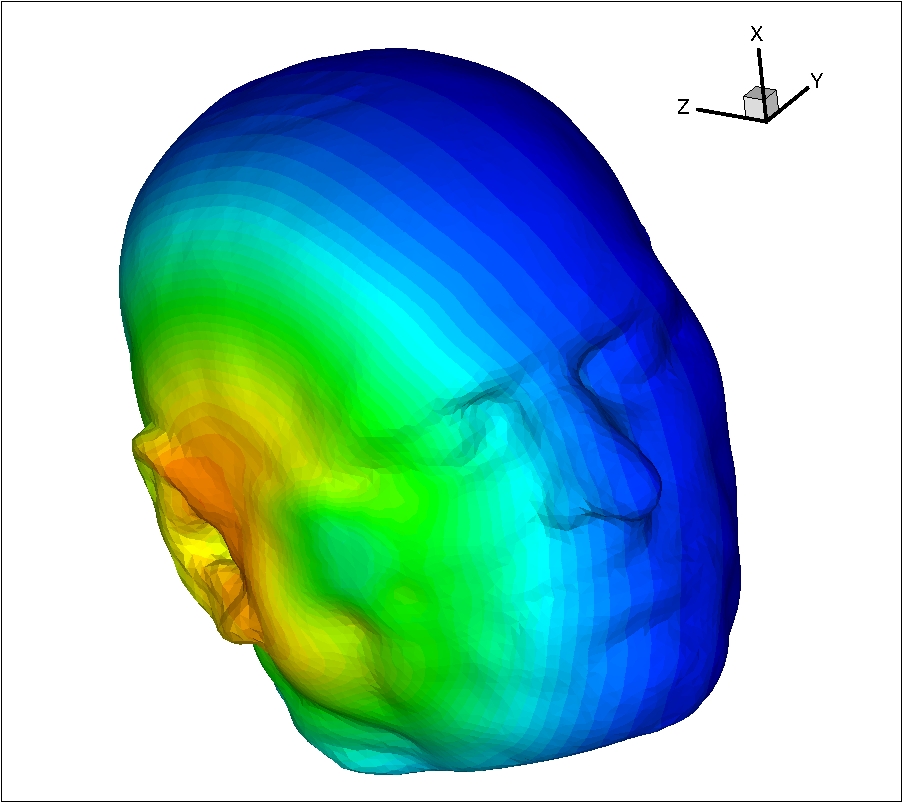
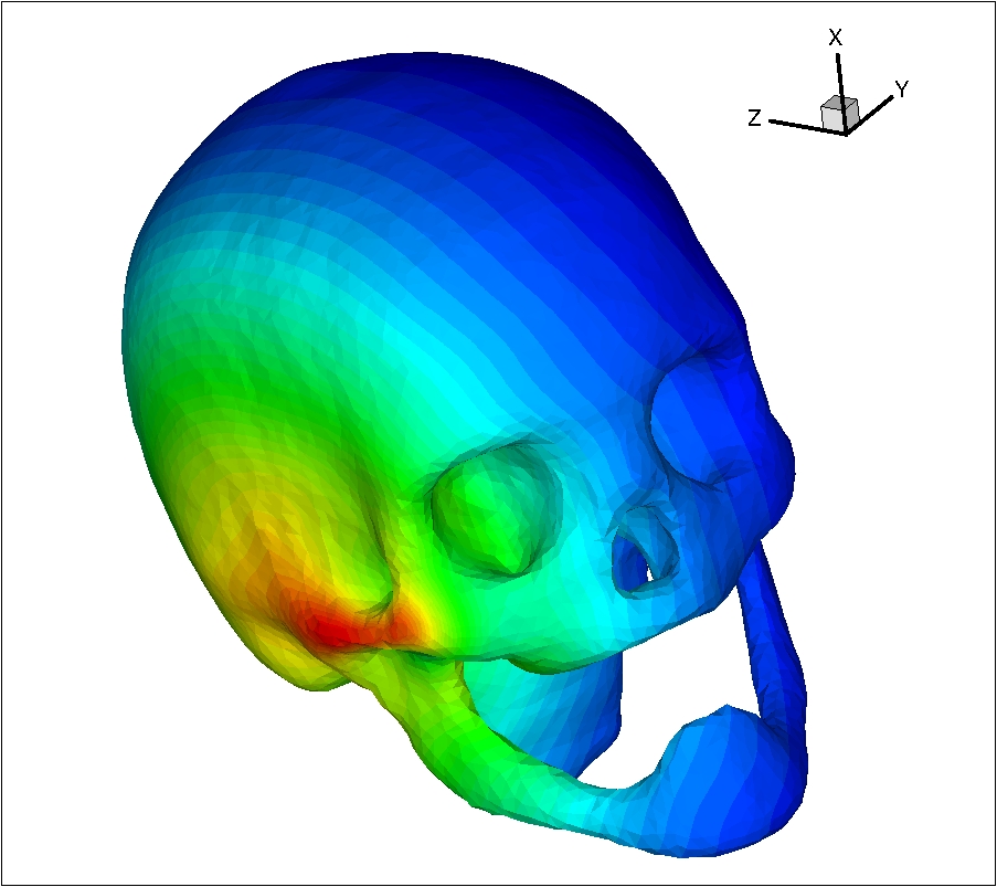
Despite the high complexity both in terms of heterogeneity and geometrical features of tissues, the great majority of numerical studies so far have been conducted using variants of the widely known FDTD (Finite Difference Time Domain) method due to Yee [63] . In this method, the whole computational domain is discretized using a structured (cartesian) grid. Due to the possible straightforward implementation of the algorithm and the availability of computational power, FDTD is currently the leading method for numerical assessment of human exposure to electromagnetic waves. However, limitations are still seen, due to the rather difficult departure from the commonly used rectilinear grid and cell size limitations regarding very detailed structures of human tissues. In this context, the general objective of the contributions of the NACHOS project-team is to demonstrate the benefits of high order unstructured mesh based Maxwell solvers for a realistic numerical modeling of the interaction of electromagnetic waves and biological tissues with emphasis on applications related to numerical dosimetry. Since the creation of the team, our works on this topic have mainly been focussed on the study of the exposure of humans to radiations from mobile phones or wireless communication systems (see Fig. 1 ). This activity has been conducted in close collaboration with the team of Joe Wiart at Orange Labs/Whist Laboratory http://whist.institut-telecom.fr/en/index.html (formerly, France Telecom Research & Development) in Issy-les-Moulineaux [15] .
|
Interaction of electromagnetic waves with nanoparticles at optical frequencies (nanophotonics).
Nanostructuring of materials has opened up a number of new possibilities for manipulating and enhancing light-matter interactions, thereby improving fundamental device properties. Low-dimensional semiconductors, like quantum dots, enable one to catch the electrons and control the electronic properties of a material, while photonic crystal structures allow to synthesize the electromagnetic properties. These technologies may, e.g., be employed to make smaller and better lasers, sources that generate only one photon at a time, for applications in quantum information technology, or miniature sensors with high sensitivity. The incorporation of metallic structures into the medium add further possibilities for manipulating the propagation of electromagnetic waves. In particular, this allows subwavelength localisation of the electromagnetic field and, by subwavelength structuring of the material, novel effects like negative refraction, e.g. enabling super lenses, may be realized. Nanophotonics is the recently emerged, but already well defined, field of science and technology aimed at establishing and using the peculiar properties of light and light-matter interaction in various nanostructures. Nanophotonics includes all the phenomena that are used in optical sciences for the development of optical devices. Therefore, nanophotonics finds numerous applications such as in optical microscopy, the design of optical switches and electromagnetic chips circuits, transistor filaments, etc. Because of its numerous scientific and technological applications (e.g. in relation to telecommunication, energy production and biomedicine), nanophotonics represents an active field of research increasingly relying on numerical modeling beside experimental studies.
Plasmonics is a related field to nanophotonics. Nanostructures whose optical scattering is dominated by the response of the conduction electrons are considered as plasmomic media. If the structure presents an interface with e.g. a dielectric with a positive permittivity, collective oscillations of surface electrons create surface-plasmons-polaritons (SPPs) that propagate along the interface. SPPs are guided along metal-dielectric interfaces much in the same way light can be guided by an optical fiber, with the unique characteristic of subwavelength-scale confinement perpendicular to the interface. Nanofabricated systems that exploit SPPs offer fascinating opportunities for crafting and controlling the propagation of light in matter. In particular, SPPs can be used to channel light efficiently into nanometer-scale volumes, leading to direct modification of mode dispersion properties (substantially shrinking the wavelength of light and the speed of light pulses for example), as well as huge field enhancements suitable for enabling strong interactions with nonlinear materials. The resulting enhanced sensitivity of light to external parameters (for example, an applied electric field or the dielectric constant of an adsorbed molecular layer) shows great promise for applications in sensing and switching. In particular, very promising applications are foreseen in the medical domain [49] - [64] .
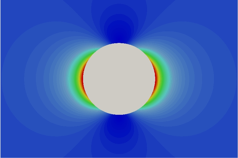
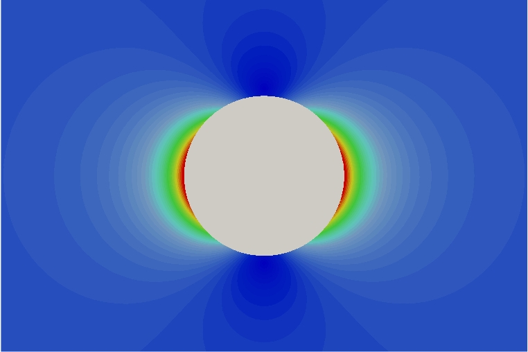
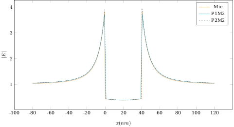
Numerical modeling of electromagnetic wave propagation in interaction with metallic nanostructures at optical frequencies requires to solve the system of Maxwell equations coupled to appropriate models of physical dispersion in the metal, such the Drude and Drude-Lorentz models. Her again, the FDTD method is a widely used approach for solving the resulting system of PDEs [60] . However, for nanophotonic applications, the space and time scales, in addition to the geometrical characteristics of the considered nanostructures (or structured layouts of the latter), are particularly challenging for an accurate and efficient application of the FDTD method. Recently, unstructured mesh based methods have been developed and have demonstrated their potentialities for being considered as viable alternatives to the FDTD method [54] - [56] - [47] . The activities of the NACHOS project-team towards the development of accurate and efficient unstructured mesh based methods for nanophotonic applications have started in 2012 and are conducted in collaboration with Dr. Maciej Klemm at University of Bristol who is designing nanoantennas for medical applications [55] .
|
||
|


